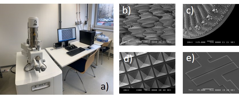
Equipment: JEOL JSM-IT 100
Technique: Scanning Electron Microscopy (SEM)
Contact person (Joanneum Research): Barbara Stadlober (barbara.stadlober@joanneum.at)
Responsible: Herbert Gold (herbert.gold@joanneum.at)
Description: The JEOL JSM-IT 100 is a compact SEM designed for fast imaging. In SEM a cathode ray focused to nm size is scanned over a sample where it is both reflected and knocking secondary electrons out of the material. Either secondary or reflected electrons, are collected by the detector and the current of these electrons is displayed as brightness in the generated image. The resolution is far better than in optical microscopy and less than in scanning probe methods. A vital advantage is it’s exceptional depth of focus that enables a vivid 3D impression of images.
Specifications:
- Maximum Sample size: max diameter 80 mm; max height 35 mm;
- Sample loading and unloading time: ≤ 4 minutes;
- Resolution: nominal (diam. e-beam) 4nm, in practice features down to ≈100nm resolved (reasonable magnification x30.000 at 128mm x 96mm image), depends heavily on sample. Requests of customers are checked individually.
- Accelerating Voltage: 0.5 to 20 kV.
- Sample manipulation (stage): Tilt -10° to 90° ; rotation 360° ; movement: 80 x 40 mm.
Constraints for samples:
- must be conductive or made conductive by sputtering;
- must be suitable for high vacuum of 10-6 to 10-7 mbar;
- should withstand the impact of the electron beam (up to 20 kV, 10 pA to 10 nA);
Suitable Samples:
All samples fulfilling the constraints can be imaged. That is in particular: Si and metals, ceramics if (made) conductive and not porous, biological materials after being dried and metal coated.
Note: A higher resolution SEM is available at JOR-MAT, where the sample loading and unloading takes 20 to 40 minutes (see description of E-Line equipment).
