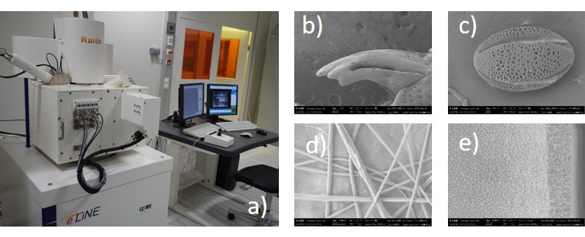
Equipment: RAITH/e-line
Technique: Electron Beam Lithography, Scanning Electron Microscope
Contact person (Joanneum Research): Barbara Stadlober (barbara.stadlober@joanneum.at)
Responsible: Philipp Schäffner (philipp.schaeffner@joanneum.at)
Description: Electron beam lithography (EBL) is a method for creating ultra-fine, nanometer-sized structures in modern nanotechnology. It is an important instrument in semiconductor technology, used to produce photomasks for photolithography, or stamps for other lithographic processes. The EBL is based on the conventional scanning electron microscope (SEM), but rather than scanning over the sample line by line as is the case for imaging, the beam path is defined by the structural geometry. Accordingly, it is a very flexible, albeit expensive, serial process.
One major benefit of the EBL is its very high resolution, which is not limited by diffraction. This is used in semiconductor technology to produce nanostructures on silicon: for this purpose, the silicon is first covered with a thin layer of photoresist, which is then structured by the electron beam. The structured photoresist is partially removed by development and the inscribed pattern is subsequently transferred to the silicon through etching. Besides, the integrated SEM can be used for high-resolution imaging of nanometer-sized features.
Specifications:
| Max. sample size | 100 mm × 100 mm (4” wafer) on flat sample holder 20 mm × 20 mm on tiltable / rotatable stage |
||
| Max. sample height | 20 mm | ||
| Max acceleration voltage | 30 kV | ||
| Max aperture size | 30 µm | ||
| Emitter type | Thermionic (tungsten emitter | ||
| SEM Column | Zeiss Gemini | ||
| Stage | Laser Interferometer Stage (sub-nm alignment precision) | ||
| Lithography resolution | < 20 nm (depending on resin, substrate and feature height) | ||
| Type of samples | conductive (non-conductive surfaces have to be coated with a thin Ag/Pd layer of a few tens of nanometers) |
Link for additional information:
https://www.joanneum.at/materials/infrastruktur/elektronenstrahl-lithografie
https://raith.com/product/eline-plus/ (successor model)
