0
Wishlist

TA4.1. Device metrology & characterization

Transnational Access Activity
Countries/Institutes
More +
Mechanical peel testing machine Mark-10 with a ESM303 test stand with a series 5 force gauge and G1008 film and paper grip.
Two available climate chambers for controlled humidity and temperature experimentation.
Customizable measurement setups for the characterization of electrochromic displays
Advanced equipment for electrical characterization of materials, components, devices and circuits in ESD protected area (EPA).
The Anton-Paar Rheometer is a quick and convenient method to measure the rheology of inks. 
The JEOL JSM-IT 100 is a compact SEM designed for fast imaging. In SEM a cathode ray focused to nm size is scanned over...
Atomic Force Microscopy (AFM) is a high resolution scanning probe microscope with resolution on the order of sub nanometer.
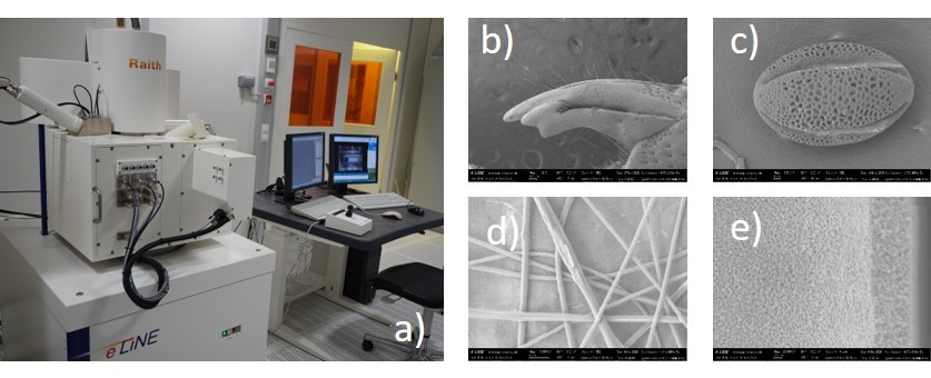
Electron beam lithography (EBL) is a method for creating ultra-fine, nanometer-sized structures in modern nanotechnology. It is an important instrument in semiconductor technology, used...
This setups allows for calibrated, reproducible measurements to evaluate the performance of ferroelectric sensors including hysteresis poling thereof.
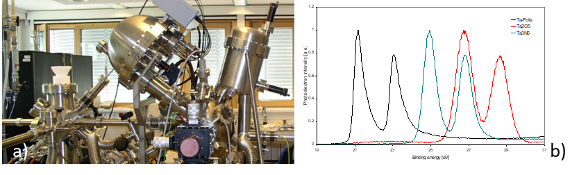
XPS is a surface sensitive method for chemical analysis widely used for e. g.  thin films, molecular layers or chemical surface modification. The sample...
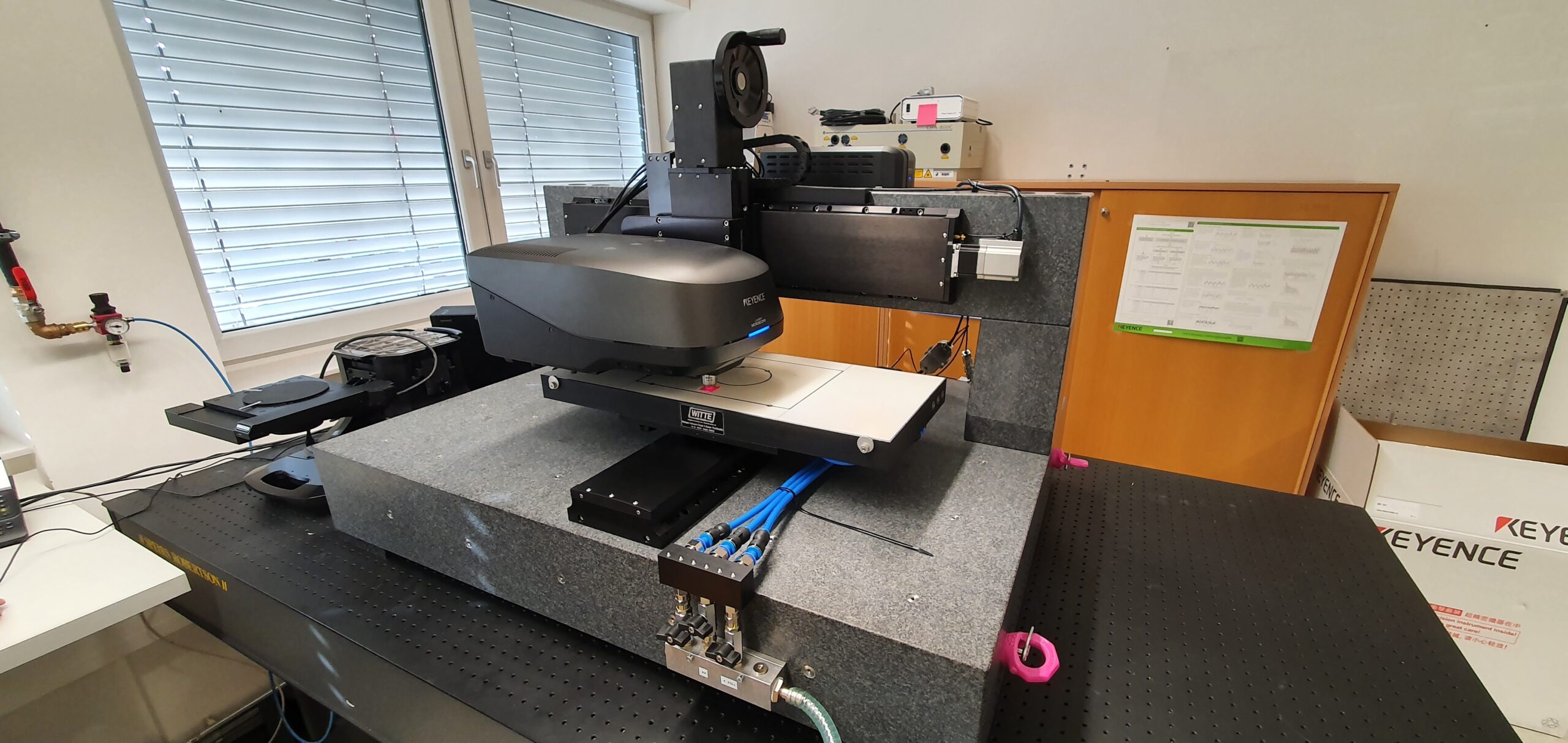
The 3D laser scanning microscope of the VK-X1050 model series uses two different measurement principles combined in one device; depending on the application, a...
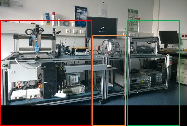
Spectroscopic ellipsometry is an optical technique using the relative phase and amplitude changes in polarized light reflected from a surface or a thin film...