0
Wishlist

Page 10

Countries/Institutes
Transnational Access Activity
Keysight 33500B is a Waveform Generator. It has two channels and allows for arbitrary waveform generation.  
Setup for I-V, C-V time dependent and pulsed-IV measurements in substrates up to 4” (2” max recommended), on cryogenic probe station with optical arm...
 A four-point-probe technique for measuring semiconductor resistivities, which is easy to implement, nondestructive, and especially convenient for probing the wafers used in device fabrication.
The OCA 15 is the R&D instrument for automated video contact angle metrology and drop shape analysis.
The HL5500PC is a high-performance Hall Effect Measurement System with a 0.5 T permanent magnet.
Setup for I-V and time dependent measurements in substrates up to 2”, at room temperature, with dark box enclosure.
Setup for I-V and time dependent measurements in substrates up to 6”, from room temperature to 300 °C, with dark box enclosure.
Zeiss Auriga combines a high-resolution SEM for imaging materials and devices at nanoscale with a FIB column enabling precise milling.
Software for modelling thin-film solar cells with arbitrary device geometry.
A suite of tools by SILVACO™ for TCAD simulation of semiconductor technologies.
Mechanical peel testing machine Mark-10 with a ESM303 test stand with a series 5 force gauge and G1008 film and paper grip.
Two available climate chambers for controlled humidity and temperature experimentation.

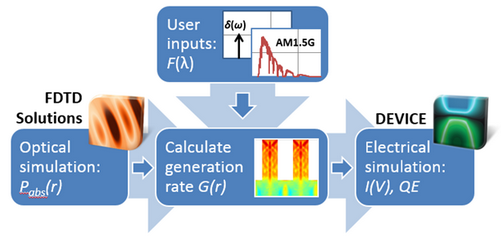
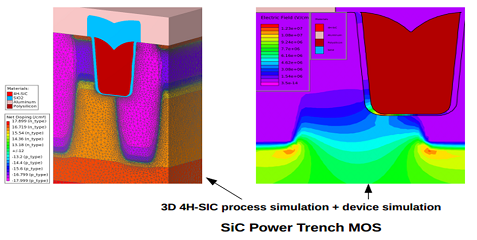
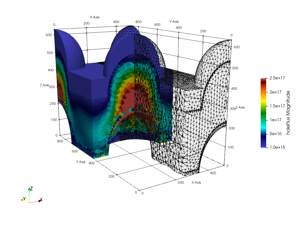
Access to design, modelling and simulation facilities will address projects oriented on high-resolution multiscale process simulations, as well as machine learning artificial intelligence based approaches giving insight and guidelines for novel material growth, functional design, and fabrication.

Access to materials synthesis and characterization facilities will be devoted to faster, cheaper and more sustainable ink/ pastes formulation with improved quality control dedicated to specific application scopes.

Access to prototypes fabrication facilities will focus on highly efficient production of sophisticated and complex flexible large-area printed electronics and photonics systems with high conformability and integrability dedicated to specific application needs allowing upscaling and technology transfer processes towards industrial production.

Access to demonstrators’ test, validation and characterization aims to establish performance and stability tests under industrial protocols in simulated and real conditions for various types of devices using a wide variety of available characterization methods aiming at specifying universal metrology protocols. Besides, it will offer solutions on encapsulation processes and investigations of ageing processes while developing automated testing setups to accelerate device evaluation.