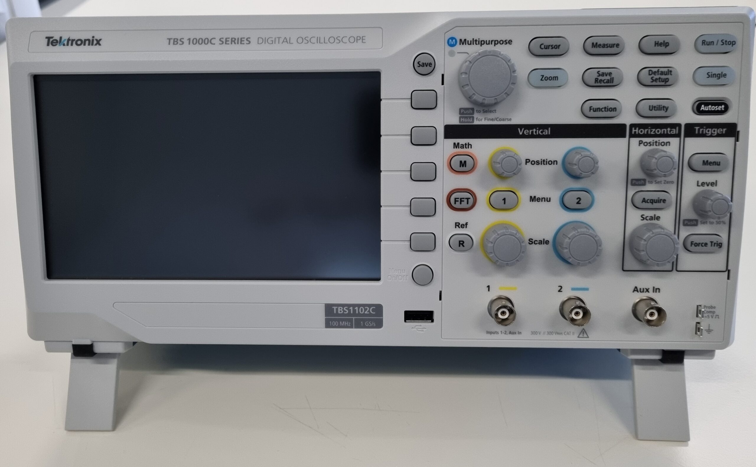
Digital storage oscilloscope is an electronic device consisting of numerous software and electronic hardware modules that allow to capture, process, view, and store electrical signals
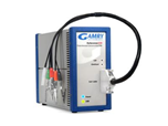
The Reference 600™ is a Potentiostat/Galvanostat/ZRA equipped with acquisition and analysis software for physical electrochemistry and electrochemical impedance experiments.
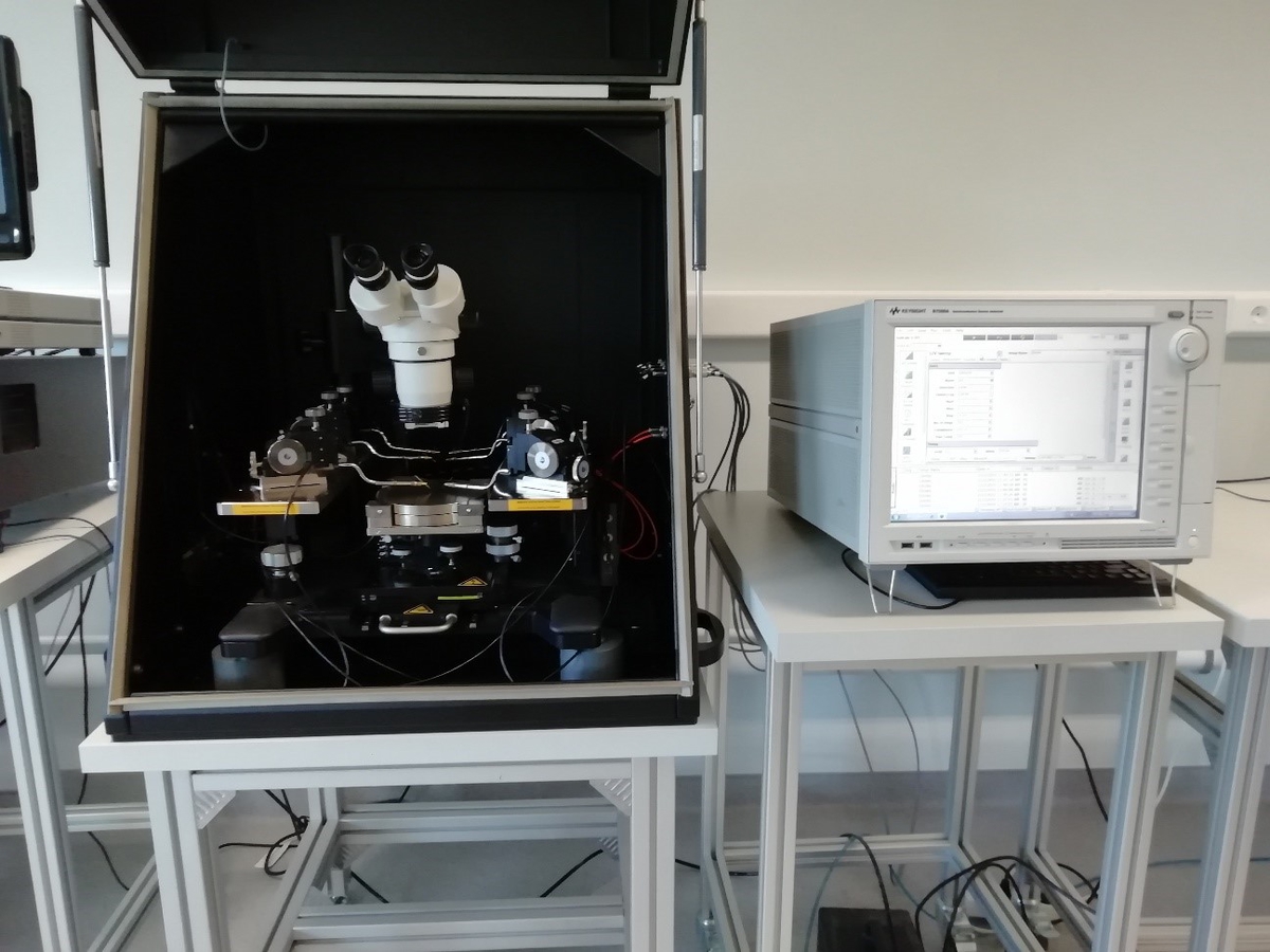
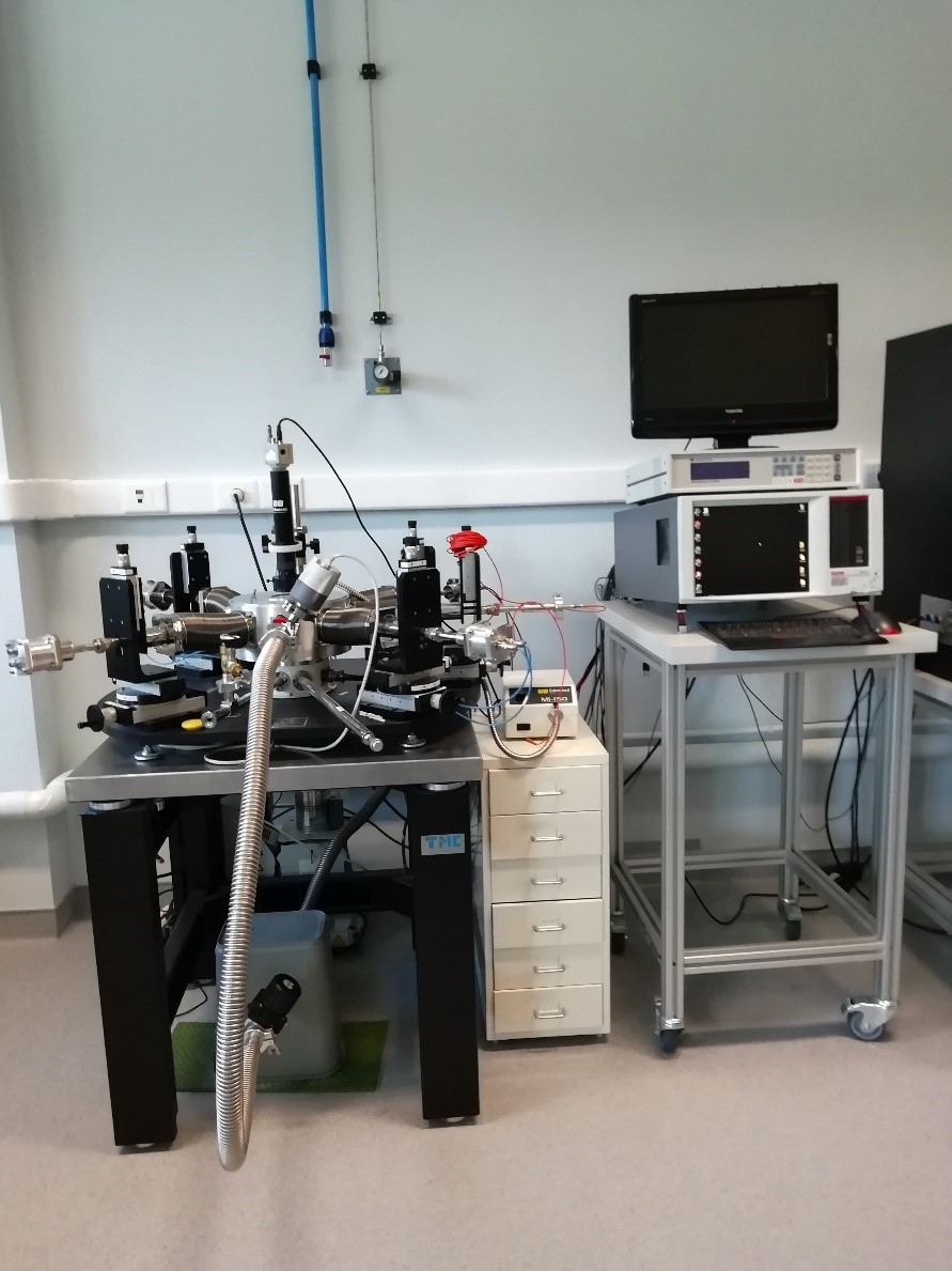
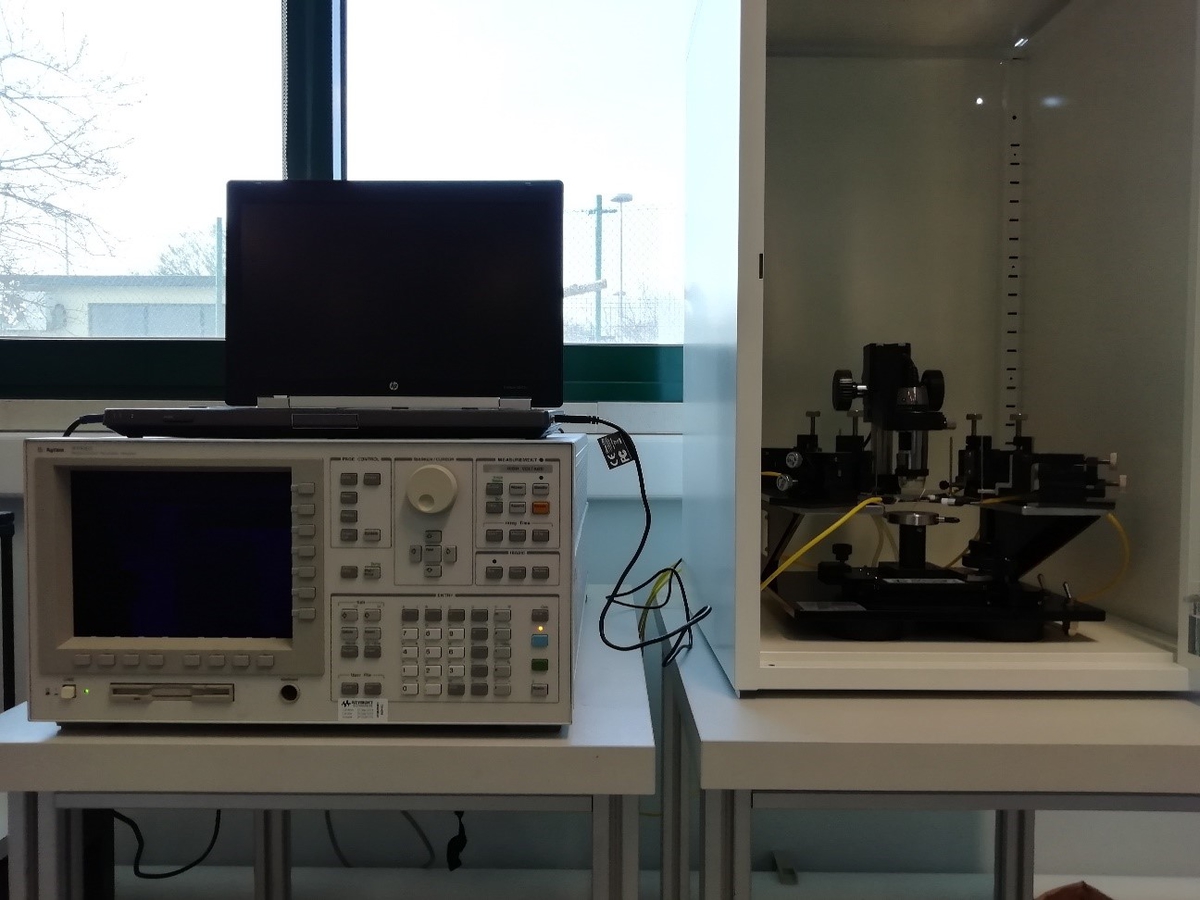
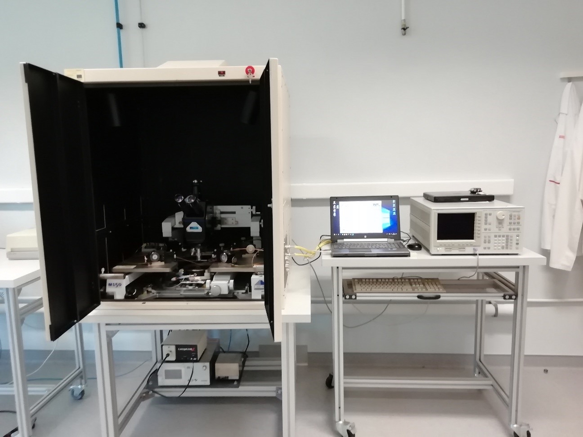
Setup for I-V, C-V time dependent and pulsed-IV measurements in substrates up to 4” (2” max recommended), on cryogenic probe station with optical arm...
We use cookies to ensure that we give you the best experience on our website. If you continue to use this site we will assume that you are happy with it.OkNoPrivacy policy